


 |
LED Car Headlights featuring input supply voltage range from 7V to 40V and single pin on off brightness control using DC voltage or PWM
Product Details:
| Place of Origin: | Dongguan,Guangdong,China |
| Brand Name: | UCHI |
| Certification: | UL.VDE,SGS,REACH,CQC,CSA.ISO.ROHS,CUL |
Payment & Shipping Terms:
| Minimum Order Quantity: | 1000PCS |
|---|---|
| Price: | Negotiable |
| Packaging Details: | Bulk |
| Delivery Time: | 5-7 days |
| Payment Terms: | T/T,Paypal,Western Union, |
| Supply Ability: | 5000,000,000PCS Per Month |
|
Detail Information |
|||
| Lumens: | 10000LM / Set | Led Chips: | Phi-lips Chips |
|---|---|---|---|
| Conditiion: | 100% Brand New | Light Power: | 160W/kit (80W/bulb) |
| Material: | Aluminum Alloy | Starting Power: | 150W |
| Key Words: | Car Headlamp | Light Lumen: | 9600LM/set |
| Aperture: | Angel's Eye | Luminous Flux: | 4000 Lumens Per Bulb |
| Working Voltage: | 9-36V DC | Model: | G5S-H4 |
| Compatibility: | Fits Most Car Models With H11/H7/H4 Sockets | Lamp Lumen: | 4000LM/Bulb |
| Product Mode: | G7-H11-PHI-4000LM | ||
| Highlight: | LED Car Headlights 7V-40V,PWM LED Car Headlights,Single Pin Brightness Control Headlights |
||
Product Description
General Description
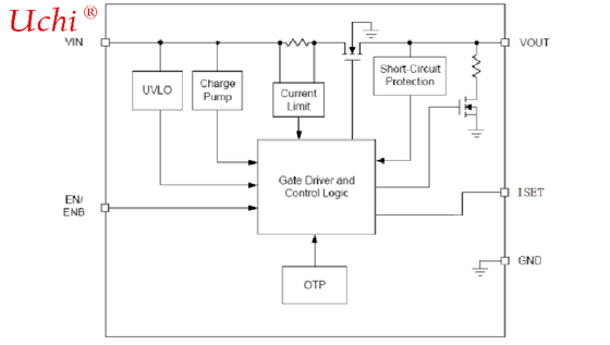
The EC9521 power switches are designed for USB applications.
The 35mΩ N-channel MOSFET power switch satisfies the voltage drop requirements of USB specification.
The protection features include current-limit protection, short-circuit protection, and over-temperature protection.
The device limits the output current at current limit threshold level.
The over-temperature protection limits the junction temperature below 140℃ in case of short circuit or over load conditions. An enable input to enable or disable the device.
Features
◆35mΩ High Side MOSFET
◆Voltage Range: 3.5V to 5.5V
◆Current-Limit and Short-Circuit Protections
◆Over-Temperature Protection
◆Iset Input
◆Enable Input
◆Lead Free and Green Devices Available
Applications
◆Notebook and Desktop Computers
◆USB Ports
◆High-Side Power Protection Switches s
Function Description VIN Under-Voltage Lockout (UVLO) The EC9521 power switches have a built-in under-voltage lockout circuit to keep the output shutting off until internal circuitry is operating properly. The UVLO circuit has hysteresis and a de-glitch feature so that it will typically ignore undershoot transients on the input. When input voltage exceeds the UVLO threshold, the output voltage starts a soft-start to reduce the inrush current. Power Switch The power switch is an N-channel MOSFET with a low RDS(ON). The internal power MOSFET does not have the body diode. When IC is off, the MOSFET prevents a current flowing from the VOUT back to VIN and VIN to VOUT. Current-Limit Protection The EC9521 power switches provide the current- limit protection function. During current-limit, the devices limit output current at current limit threshold. For reliable operation, the device should not be operated in current-limit for extended period. Short-Circuit Protection When the output voltage drops below 1.5V, which is caused by an over-load or a short-circuit, the devices limit the output current down to a safe level. The short-circuit current limit is used to reduce the power dissipation during short-circuit conditions. If the junction temperature reaches over-temperature threshold, the device will enter the thermal shutdown. ISET ISET pin can set the current limit by Riset: ILim=120k*1.14V/Riset Enable/Disable Pull the EN below 0.8V will disable the device, and pull EN above 2V will enable the device. When the IC is disabled, the supply current is reduced to less than 1μA. The enable input is compatible with both TTL and CMOS logic levels. The EN pin cannot be left floating. Over-Temperature Protection When the junction temperature exceeds 140℃, the internal thermal sense circuit turns off the power FET and allows the device to cool down. When the device’s junction temperature cools by 20℃, the internal thermal sense circuit will enable the device, resulting in a pulsed output during continuous thermal protection. Thermal protection is designed to protect the IC i n the event of over temperature conditions. For normal operation, the junction temperature cannot exceed TJ=+125℃.
Application Information Input Capacitor A 1μF ceramic bypass capacitor from VIN to GND, located near the EC9521, is strongly recommended to suppress the ringing during short circuit fault event. Without the bypass capacitor, the output short may cause sufficient ringing on the input (from supply lead inductance) to damage internal control circuitry. Output Capacitor A low-ESR 10μF aluminum electrolytic or tantalum between VOUT and GND is strongly recommended to reduce the voltage drop during hot-attachment of downstream peripheral. (Per USB 2.0, output ports must have a minimum 120μF of low-ESR bulk capacitance per hub). Higher-value output capacitor is better when the output load is heavy. Additionally, bypassing the output with a 0.1μF ceramic capacitor improves the immunity of the device to short-circuit transients. Layout Consideration The PCB layout should be carefully performed to maximize thermal dissipation and to minimize voltage drop, droop and EMI. The following guidelines must be considered: 1.Please place the input capacitors near the VIN pin as close as possible. 2.Output decoupling capacitors for load must be placed near the load as close as possible for decoupling high frequency ripples. 3.Locate EC9521 and output capacitors near the load to reduce parasitic resistance and inductance for excellent load transient performance. 4.The negative pins of the input and output capacitors and the GND pin must be connected to the ground plane of the load. 5.Keep VIN and VOUT traces as wide and short as possible.
