


 |
SMD Varistor with High Peak Reverse Voltage Rated for Effective DDR5 16Gb A-Die SDRAM
Product Details:
| Place of Origin: | Dongguan,Guangdong,China |
| Brand Name: | UCHI |
| Certification: | SGS.MA.CTI.CQC |
| Model Number: | DDR5 16Gb A-Die SDRAM |
Payment & Shipping Terms:
| Minimum Order Quantity: | 10000PCS |
|---|---|
| Price: | Negotiable |
| Packaging Details: | Bulk/Tape |
| Delivery Time: | 5-7 days |
| Payment Terms: | T/T,Paypal,Western Union, |
| Supply Ability: | 5000,000,000PCS Per Month |
|
Detail Information |
|||
| Production Series: | SMD Varistor | Maximum Current: | Varies (e.g., Up To Several Amperes) |
|---|---|---|---|
| Technology: | Metal Oxide | Energy Absorption: | Typically 0.1J To 10J |
| Applications: | Surge Protection In Electronic Circuits | Voltage Rating Dc: | 385V |
| Good Name: | SMD Varistor 10D471K 470V 10% | Energy Resistance: | A 0.02J B 0.05J |
| Insulation Resistance: | Typically >100 MΩ | Terminal: | Special SMT Mount |
| Storagetemperature: | -55 +125 | Varistor Voltage Ac: | 175-385V |
| Varistor Voltage: | 470V+/-10% | ||
| Highlight: | SMD Varistor for DDR5 SDRAM,High peak reverse voltage varistor,SMD Varistor with A-Die compatibility |
||
Product Description
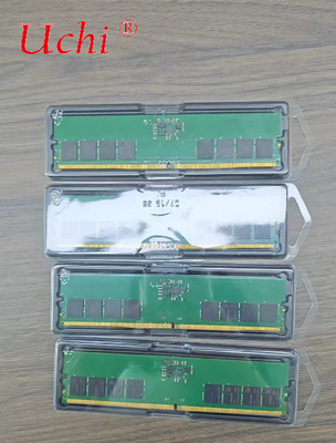
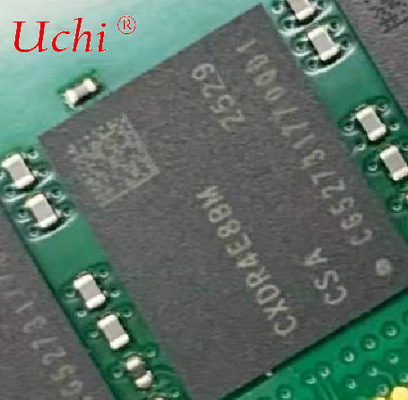
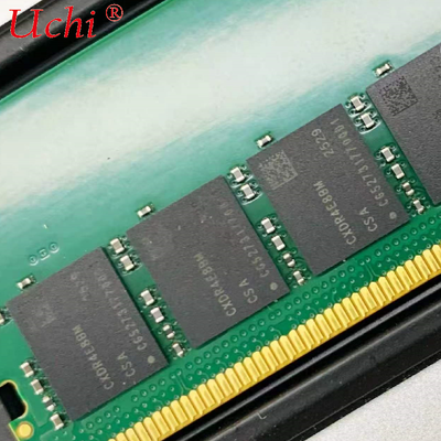
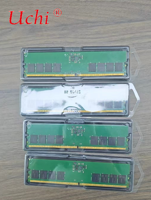
DDR5 16Gb A-Die SDRAM
1.1 Key Features
• JEDEC Standard Compliant;
• Power Supply: VDD/VDDQ = 1.1V (1.067V (-3%) to 1.166V (+6%));
• Power Supply: VPP = 1.8V (1.746V (-3%) to 1.908V (+6%));
• JEDEC standard package: 82-ball FBGA for x4/x8, 102-ball FBGA for x16;
• Array Configuration:
• 32banks(8 bank groups, 4 banks for each bank group) for x4/x8;
• 16banks(4 bank groups, 4 banks for each bank group) for x16;
• 16n-bit prefetch architecture;
• Burst Length (BL): BL16, BC8 OTF, BL32(Optional), BL32 OTF(Optional) are supported; • Programmable CAS Latency (CL);
• Programmable CAS Write Latency (CWL);
On-Die Termination (ODT) via Mode Register setting: RTT_PARK, RTT_WR, RTT_NOM_WR, RTT_NOM_RD, DQS_RTT_PARK
Same Bank Refresh and All Bank Refresh for Normal Refresh Mode and Fine Granularity Refresh Mode; • Fine granularity refresh 2x (0°C ≤ TCase ≤ 85°C), 4x (85°C ≤ TCase ≤ 95°C) mode for smaller tRFC;
• Bi-directinal Differential Data-Strobe;
• POD(Pseudo Open Drain) interface for data input/output, command and address input;
• Connectivity Test Mode(TEN) is supported;
• Internal VREF for data inputs, command/address inputs and chip select;
• CAI(Command Address Inversion);
• 1N/2N Mode is supported for Commands;
• 4-tap Decision Feedback Equalizer(DFE) is supported;
• Loopback and bit Error Rate Test are supported;
• hPPR/sPPR is supported; sPPR Do/undo/Lock is supported;
• Training Modes:
• VrefDQ / VrefCA / VrefCS Training
• Read Training Mode
• CA Training Mode
• CS Training Mode
• Per Pin VREFDQ Training
• Write Leveling Training Mode
• Duty Cycle Adjuster (DCA) for Read - Global
• Per Pin DCA(Duty Cycle Adjuster) for Read - Per Pin(DQ) • Per DRAM Addressability (PDA);
• Maximum Power Saving Mode (MPSM);
• Multi-Purpose Command (MPC);
• Asynchronous reset for power up;
Operating case temperature: 0°C ≤ TCase ≤ 95°C;
• Support auto-refresh and self-refresh mode;
• Average Refresh Period:
• 3.9 μs/32ms, 8K cycles at 0°C ≤ TCase ≤ 85°C; • 1.95 μs/16ms, 8K cycles at 85°C < TCase ≤ 95°C;
Programmable Read/Write preambles and postambles;
• Cyclic Redundancy Code (CRC) is supported for Read/Write Data Integrity; • On-Die ECC;
• ECC Transparency and Error Scrub;
• MBIST / mPPR;
• Gear Down Mode is not supported;
• Package Output Driver Test Mode;
• Partial Array Self Refresh(PASR) is not supported;
• RoHS compliant
Note:
The functionality described and the timing specifications included in this datasheet are for the DLL Enabled mode ofoperation (normal operation), unless specifically stated otherwise.
DDR5 SDRAM Package Specifications
This chapter will mainly introduce the package dimension and ballout in x4/x8/x16 configurations which may help to match your device.
DDR5 SDRAM Package Dimension on Page 7
• DDR5 SDRAM x8 Ballout Using MO-210-AN – 82-ball on Page 8 • Pinout Description on Page 9
Want to Know more details about this product
