


|
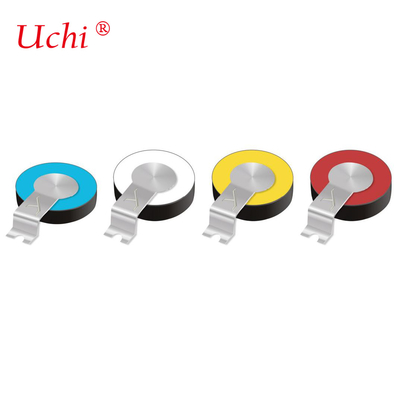
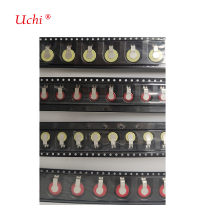
SMD Surface Mount Varistors , SMT Metal Oxide Varistor MOV MOVS
Product Details:
| Place of Origin: | Dongguan,Guangdong,China |
| Brand Name: | UCHI |
| Certification: | CQC,UL,TUV,SGS,SVHC |
| Model Number: | 2012 |
Payment & Shipping Terms:
| Minimum Order Quantity: | 4000PCS/ |
|---|---|
| Price: | Negotiable |
| Packaging Details: | Bulk/Tape |
| Delivery Time: | 5-7 days |
| Payment Terms: | T/T,Paypal,Western Union,Money gram |
| Supply Ability: | 5000,000,000PCS Per Month |
|
Detail Information |
|||
| Maxi Mum Static Power: | 0.1W,0.25W,0.4W | Leakage Current: | ≤20uA |
|---|---|---|---|
| Certificati On Temperat Ure (℃): | -40~125 | Relative Humidity: | ≤95% |
| Atmospheric Pressure: | 86~106Kpa | Vibration Frequency: | 10~50HZ |
| Acceleration: | 98m/S² | Storage Temperature: | -40~85℃ |
| Highlight: | SMT Surface Mount Varistors,MOV Surface Mount Varistors,MOVS Voltage Dependent Resistor |
||
Product Description
SMD Varistor Surface Mount Varistors SMT Metal Oxide Varistor MOV SMD MOVS voltage dependent resistor
I. Dimensions, Appearance Identification and Packaging (mm)
1,In the drawing buard, it is suggested to regard A solder joint as Lline, B solder joint as N line, and wire the copper foih counected widl B solder joint around the pressure sensitive chip (the whole dliameter D should be regarded as belonging to A solder joint).
2,For the sake of safety arcing, the circular edge of the chip shall be at least 2.5mm away from any other conductive devices,as shown in the figure above (in order to prevent mutual displacement between the chip and other devices, if space permits, the larger the space, the better)
3,There are unfavorable factors in the use of varistor in DC circuit.It is not recommended to use varistor in DC circuit
after rectification. Please consider it carefully or contact our company telephone 13925862052 directly. Thank you!
|
Model JYVDR~ |
Pad A |
Pad B |
center distance |
Diameter |
Height ± 1.0 |
Thickness |
Coating material andremarks (insulating paint) |
||
| Φa | b1 | b2 | |||||||
| 05D271 |
2.7
3.3
4.0 |
3.5
3.8
4.0 |
2.5
2.5
2.5 |
5.75
6.75
8.25 |
5.0
7.0
10.0 |
9.1
11.1
14.2 |
2.0 |
Blue 271 :270VDC±10%; White 471 :470VDC±10%; Yellow 511: 510VDC±10%; Red 561 :560VDC±10% 15 |
|
|
05D471 05D511
07D271 |
3.0
2.0 |
||||||||
|
07D471 07D511 07D561
10D271 |
3.0
2.0 |
||||||||
|
5D271 5D7D271 7D 10D271 10D |
4000PCS; 3000PCS; 3000PCS. 2000PCS; 2000PCS. 1500PCS; |
||||||||
| 10D471 10D511 10D561 |
3.0 |
||||||||
|
05 07 10D all series adopt 15 inch reel and 24 inch Fee der placement machine |
|||||||||
![]()
Electrical Performance
|
Series/M odel
JYVDR~ |
Pressure Sensitive Resistance VDC |
Maximum Allowable Circuit Pressure |
(8/20us) Maximum Limiting Pressure (8/20us) |
Maximum Circulation Energy Combined wave |
Maxi mum Static Power |
Electric Capacity |
Leakage Current |
Certificati on Temperat ure (℃) |
VI Charact eristic Curv |
Pulse Deratin g Curve |
||
| VAC | VDC | VDC | AIp | A | W | pF |
≤20uA |
-40~ 125 |
Attach ment I |
Attach ment II |
||
| 05D271 | 270±10% | 170 | 220 | 480 | 8A |
500A (1000V) |
0.1 |
100 | ||||
| 05D471 | 470±10% | 300 | 380 | 810 |
10A |
65 | ||||||
| 05D511 | 510±10% | 325 | 415 | 870 | 60 | |||||||
| 07D271 | 270±10% | 170 | 220 | 450 | 15A |
1.0KA (2000V) |
0.25 |
170 | ||||
| 07D471 | 470±10% | 300 | 380 | 770 |
20A |
115 | ||||||
| 07D511 | 510±10% | 325 | 415 | 840 | 110 | |||||||
| 07D561 | 560±10% | 350 | 450 | 925 | 100 | |||||||
| 10D271 | 270±10% | 170 | 220 | 450 | 35A |
2.0KA (4000V) |
0.40 |
380 | ||||
| 10D471 | 470±10% | 300 | 380 | 760 |
40A |
250 | ||||||
| 10D511 | 510±10% | 325 | 415 | 835 | 230 | |||||||
| 10D561 | 560±10% | 350 | 450 | 920 | 210 | |||||||
For different voltage application environments, we recommend the following pressure sensitive combinations to provide overvoltage, surge and lightning stroke protection for ACLED.
| Working Voltage Environment |
Last-level Pressure Sensitive Parameter |
Next-level Pressure Sensitive Parameter |
Remarks |
|
110VAC±20% |
270VDC±10% |
. Tow levels of pressure sensitive combinations can be improved to 4KV lightning protection; user can select pressure sensitive volume as needed. | |
|
220-230VAC±20% |
510VDC±10% |
470VDC±10% |
|
|
240VAC±20% |
560VDC±10% |
510VDC±10% |
The combination is recommended for users in Indian and Brazil. |
Since pressure sensitive resistor is easy to degrade under the environment with strong voltage fluctuation, it is required to select the combination with high pressure sensitive voltage value as much as possible under the premise that withstand voltage of IC (MOS tube) +lamp bead on lamp board is pretty high and that voltage has a large fluctuation area; besides, it is necessary to select pressure sensitive resistor with large circulation and volume as far as possible, without exceeding cost limit.
,Acceptance
Sampling should follow GB2828-87 and this Specification.
| Item | IL | AQL |
| 4- 1 Appearance, Dimension and Logo | II | 0.65 |
| 4-2 Pressure Sensitive Voltage | II | 0.65 |
| 4-3 Electric Capacity | S-3 | 0.65 |
| 4-4 Weldability | S-3 | 2.5 |
Using Environment Condition
| Environment Temperature | -40~125℃ |
|
Relative Humidity |
≤95% |
|
Atmospheric Pressure |
86~106Kpa |
|
Vibration Frequency |
10~50HZ |
|
Acceleration |
98m/S² |
|
Storage Temperature |
-40~85℃ |
Curve diagram of wave soldering
![]()
The figure above shows the general trend of reflow soldering furnace temperature curve in the market. Our chip varistors use silver electrode of porcelain body as one of the welding electrodes. Please pay attention to the setting of furnace temperature and time (if the maximum temperature is 260℃, please note that the time is 3-8s. If it exceeds 30s, the protection effect of the chip varistors will be affected)
| Item | Technical Requirement | Testing Condition and Method |
|
4- 1Appearance |
No obvious bubble, pinhole and other defects; no any visible damage lowering using performance; clear and long-lasting sign |
Visual inspection |
|
4-2Weldability |
Tin is uniform in tin immersion part; tinned area is ≥90%. |
Soak pressure sensitive resistor into 235℃±5℃ tin soldering liquid for 2±0.5 s; then take it out and observe its appearance. |
|
4-3 Resistance to Soldering Heat |
Change rate of pressure sensitive voltage before and after test is ≤±5%. |
Soak wire of pressure sensitive resistor into 350℃ ±10℃tin soldering liquid, with soak depth for 2-0.5 mm far away from pedestal. Adopt 1.5±0.2 mm thermal insulation layer and keep it for 5±0.5 s; measure pressure sensitive voltage with recovery time within 1 h-2 h. |
|
4-4High Temperature Load |
Before and after test, change rate of pressure sensitive voltage is ≤±10%; change rate of limiting voltage ≤±20%. |
Put pressure sensitive resistor in 125±2℃ for 1,000 h and apply corresponding allowable using AC pressure of the temperature; power on for 90 min and power off for 30 min. After taking pressure sensitive resistor out, put it under normal temperature for more than 1 h; measure pressure sensitive voltage and limiting voltage within 4 h. |
| 4-5 Outlet Terminal Strength |
Change rate of pressure sensitive voltage before and after test is ≤±5%. |
Apply tension to outlet terminal axis and make it act in sample main body direction; apply 10N load for 10 . |
Points for attention:
1.The accumulated error of any continuous 10 ratchet holes shall not exceed ± 0.2mm;
2 ,The non parallel distance of 250 mm in the length direction of the carrier belt shall not exceed 1 mm;
3 , The R angle of undeclared is 0.2-0.3, and the stripping angle of undeclared is 5 °;
4 , Comply with EIA-481-d and ROHS requirements;
5 , Thickness: 0.30 ± 0.05mm;
6 ,05 07 10D all series adopt 15 inch reel and 24 inch Feeder placement machine.
Appendix I: Form of VI Characteristic Curve
|
Current Model Voltage |
10-3 |
10-2 |
10- 1 |
100 |
101 |
102 |
103 |
| 05D271 | 270 | 330 | 380 | 420 | 490 | 580 | / |
| 05D471 | 470 | 580 | 640 | 720 | 840 | 1020 | / |
| 05D511 | 510 | 640 | 700 | 780 | 900 | 1120 | / |
| 05D561 | 560 | 700 | 740 | 800 | 950 | 1200 | / |
| 07D271 | 270 | 320 | 370 | 390 | 440 | 520 | 720 |
| 07D471 | 470 | 560 | 620 | 670 | 760 | 900 | 1100 |
| 07D511 | 510 | 620 | 680 | 720 | 820 | 960 | 1250 |
| 07D561 | 560 | 660 | 700 | 740 | 850 | 1050 | 1290 |
| 10D271 | 270 | 310 | 360 | 380 | 430 | 500 | 640 |
| 10D471 | 470 | 540 | 600 | 650 | 740 | 820 | 1050 |
| 10D511 | 510 | 600 | 650 | 700 | 790 | 880 | 1190 |
| 10D561 | 560 | 610 | 660 | 710 | 830 | 930 | 1260 |
附件二: Appendix II: Form of Pulse Derating Curv
|
Specificati on/Model |
Pulse Width |
50us |
100us |
500us |
|||||||||
| Current |
5A |
10A |
50A |
100A |
5A |
10A |
50A |
100A |
5A |
10A |
50A |
100A |
|
| 05D |
Times |
104 | 102 | X | X | 102 | 10 | X | X | 10 | X | X | X |
| 07D | 106 | 104 | 2 | X | 105 | 103 | X | X | 102 | 2 | X | X | |
| 10D |
∞ |
∞ |
103 | 10 |
∞ |
105 | 102 | 2 | 106 | 103 | 1 | X | |
| 14D |
∞ |
∞ |
104 | 103 |
∞ |
106 | 103 | 102 | 106 | 104 | 2 | 1 | |
| 20D |
∞ |
∞ |
105 | 104 |
∞ |
∞ |
104 | 103 |
∞ |
106 | 103 | 101 | |
Please see the specification